
Scanning Tunneling Microscope, STM
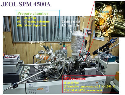
The JEOL ultra-high vacuum scanning probe microscope (UHV-SPM, JSPM 4500A) is designed and manufactured by the Japan Electron Optics Laboratory, Inc. The system consists of a main instrument, a set of pumps, a power supply unit, and a computer controller.
工作原理:
Through the tunneling effect, STM can obtain a current between an extremely sharp tip and the sample by simply applying a voltage between both of them. Although the tunneling effect is classically forbidden, it is already considered since the early development of quantum mechanics and observed in the beginning of the 1960’s. Notably, a tunneling current can be detected before tip and sample contact each other, which is held constant by treating it in an electrical feedback loop that compares it to a preset current and then varies the distance between tip and sample.

By moving the tip towards or away from the sample, the tip height is determined by the local geometric and electronic structure (Local density of states LDOS) of the surface and therefore produces a surface map in real space.
研究方向:
1.Topological systems:
Topological phases in condensed matter systems have attracted intense worldwide research interest in the past decade. Among these novel phases, quantum spin Hall (QSH) insulators or so-called two-dimensional (2D) topological insulators (TI), which host exotic surface electronic structure, are promising to be applied to build next-generation low-power spintronic devices. Three-dimensional (3D) TI feature a bulk energy gap and time-reversal symmetry-protected gapless surface states originating from spin-orbit coupling (SOC), which is distinct from the conventional band insulator. The Dirac fermions on the surface of a TI possess a definite chirality, which is associated with the one-to-one electron spin and momentum locking, resulting in a nontrivial quantum Berry phase that suppresses the back-scattering and localization of carriers.

Recently, we report the preparation of Bi (111) bilayers with uniform and flat surfaces with a top-down method using deliberate atomic-hydrogen etching. With a STM and XPS in-situ, the atomic view and the mechanism according to which hydrogen reacts with Bi2Se3 are revealed. The results show that the removal of Se elements begins from the top and bottom of a quintuple layer, leading to the formation of Bi (111) bilayers in the van der Waals gap. ARPES record in-situ and complementary DFT calculations show that a large Rashba splitting exists, which is attributed to the large SOC and potential gradient at the interface between Bi (111) BL and Bi2Se3. Strong hybridization between BL and the TI interface QL cause the topological surface states of Bi2Se3 to move to deeper QL to maintain a non-trivial band topology of the entire system. The band structures of the Bi (111) bilayers, dependent on thickness, have been traced with ARPES. By tuning the exposure to atomic-hydrogen etching we can directly control the band structures of the Bi bilayers. Our approaches and results not only enlighten the nature of 2D TI from 3D TI but also pave a new way to design Bi-based topological materials and devices for applications.
2.Graphene:
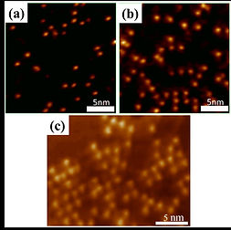
(a) Room temperature long-range interactions of bismuth adatoms (Carbon 93,180-186 (2015))
Long-range electronic interaction between Bismuth (Bi) adatoms on graphene formed on a 4H-SiC (0001) substrate are clearly observed at room temperature (T=300K). Using STM and DFT calculations, we have demonstrated that such oscillatory interaction results mainly from the mediation of graphene Dirac-like electrons and the effect of the corrugated surface of SiC substrate. These two factors cause the observed oscillatory interaction with characteristic distribution distances and linear arrangements of Bi adatoms. The present study sheds light on understanding and controlling the nucleation of adatoms and subsequent growth of nanostructures on graphene surface.


(b) Low-dimensional structures of bismuth adatoms (Sci. Rep. 5, 11623 (2015))
A series of structural transition of Bi adatoms, adsorbed on MEG, is explored at room temperature. Bi adatoms undergo a structural transition from 1D linear structures to 2D triangular islands and such 2D growth mode is affected by the corrugated substrate. Upon Bi deposition, a little charge transfer occurs and a characteristic peak can be observed in the tunneling spectrum, reflecting the distinctive electronic structure of the Bi adatoms. When annealed to ~500K, 2D triangular Bi islands aggregate into Bi nanoclusters (NCs) of uniform size. A well-controlled fabrication method is thus demonstrated. The approaches adopted herein provide perspectives for fabricating and characterizing periodic networks on MEG and related systems, which are useful in realizing graphene-based electronic, energy, sensor and spintronic devices.
研究成員:


Shu-Hsuan Su

Yuan-cheng Chi
